制造商提供单增益稳定放大器,期望抢占广阔的市场,并使学习应用设备变得很容易。但这些销售商牺牲了潜在但重要的交流性能。了解什么时候考虑非补偿运放和能够提供给你什么东西。
设计者经常想使基于传感器的系统中的振幅误差最小。这个目的经常导致放大器闭环增益的特定增益误差超过传感器频率范围。工程师通常根据其–3dB频率指定放大器带宽,但就增益精度点来看,在这个频率几乎出现30%的增益误差。所谓“有效带宽”与放大器频率响应和应用所需的增益精度有关。定义有效带宽为增益误差小于或等于指定误差的带宽。
有效带宽
传感器具有相对低频响应,频率越低,由有限开环增益产生的增益误差越小。用少于单极、闭环、频率响应模式放大器的指定值,计算有效带宽维持误差。由特定的通常如在数据手册上的增益带宽指标,计算有效带宽是可行的。放大器闭环带宽等于增益带宽除以增益,对非反转放大器完全正确,对反转放大器近似正确。
下一个考虑什么是定义最大幅度误差的基础。在所有系统中,ADC输入信号路径终端的模拟部分,通过扩充,ADC的分辨率定义了误差的影响因素。这篇文章使用ADC分辨率的½ LSB误差
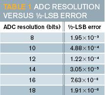
作为最大误差。随着ADC分辨率的增加,最大误差减小。表1显示了8到18位ADC分辨率的½ LSB误差。

为容易评估增益误差在频率函数中单极模式的效果,计算格式化单极函数。这个计算放置极点在1Hz,表示闭环增益降为–3dB,用理想闭环单增益或为0dB。使用这个单极模式,计算增益误差频率少于或等于给定误差。然后可以根据放大器闭环增益的–3dB带宽计算有效带宽。谨记–3dB点为几乎30%增益误差,且误差指标越小的带宽越窄。
 (1)
(1)
![]() (2)
(2)
![]() (3)
(3)
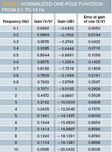
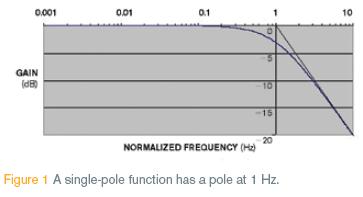
表2显示数据表计算的一部分,将增益随频率下降的趋势形象化。计算公式1~3分别随列中频率值变化(图1)。


下一步是找到特定频率,在这个频率增益误差等于指定位分辨率ADC的½ LSB。公式4为假定ADC分辨率的情况下,计算½LSB误差(表1)。
![]() (4)
(4)
为计算增益误差等于½LSB误差的频率,用公式1重新整理替代公式4,得到公式5。使用公式4和公式5计算出表3的值。
 (5)
(5)
表3中,纵向表头“频率误差”的给定频率为增益误差等于ADC分辨率的½LSB。在更低频率,增益误差小于½LSB。带宽对特定分辨率有效。例如,驱动10位ADC的放大器有效带宽为–3dB频率的0.03126,14位ADC的有效带宽为–3dB频率的0.007813。如果放大器为闭环,100kHz为–3dB频率,有效带宽分别为31.3和7.81kHz。公式1到公式5,放大器增益带宽除以其闭环增益,充分证明了放大器的有效带宽小于理论使用手册的–3dB频率。
考虑怎样在信号路径中使用放大器,能够部分减少有效带宽的迅速降低。放大器通常从传感器到ADC输入使用许多增益缩放信号。在许多情况下,增益大过10。使用放大器增益消除单增益稳定性的需求,并减少大量放大器使用的内部补偿。非补偿放大器的优点是同样功耗下增加了可用带宽和转换速率。
以上为部分翻译,英文全文:
Decompensating amplifiers improve performance
Manufacturers offering unity-gain-stable amplifiers hope to address a wide market and minimize the effort of learning to use the devices. Yet these vendors sacrifice a significant portion of the potential ac performance. Learn when to consider decompensated amplifiers and what they can offer you.
By Walter Bacharowski, National Semiconductor -- EDN, 12/3/2007
Designers often want to minimize amplitude error in sensor-based systems. This goal often leads to specifying the gain error of an amplifier’s closed-loop gain over the frequency range of the sensor. Engineers commonly specify the bandwidth of an amplifier in terms of its –3-dB frequency, but, from a gain-accuracy point of view, almost a 30% gain error occurs at this frequency. The term “effective bandwidth” connects the frequency response of the amplifier and the gain accuracy that the application requires. You define the effective bandwidth as the bandwidth for which the gain error is less than or equal to a specified error.
Effective bandwidth
Sensors have a relatively low frequency response, and, at lower frequencies, the gain error due to finite open-loop gain is small. You can calculate the effective bandwidth to maintain an error at less than a specified value from the single-pole, closed-loop, frequency-response model of the amplifier. It would be useful to calculate the effective bandwidth from specifications such as gain bandwidth that are commonly available in a data sheet. The relationship of an amplifier’s closed-loop bandwidth being equal to the gain bandwidth divided by the gain is true for noninverting amplifiers and approximately true for inverting amplifiers.
The next consideration is what basis to use in defining the maximum amplitude error. In almost all systems, the analog portion of the signal path ends at the input of an ADC, and, by extension, the resolution of the ADC defines the error of interest. This article uses an error of ½ LSB of the ADC’s resolution as the maximum error. As the resolution of the ADC increases, the maximum error decreases. Table 1 shows the ½-LSB error for ADC resolutions of 8 to 18 bits.
To easily evaluate the effect of the single-pole model on the gain error as a function of frequency, you calculate a normalized single-pole function. This calculation places the pole at 1 Hz, which represents the –3-dB loss in closed-loop gain, with an ideal closed-loop gain of one, or 0 dB. Using this single-pole model, you calculate the frequency for a gain error less than or equal to the specified error. You can then calculate the effective bandwidth in terms of the –3-dB bandwidth of the closed-loop gain of the amplifier you are evaluating. Keep in mind that the –3-dB point is almost a 30% gain error and that the bandwidth is smaller with a lower error specification.
 (1)
(1)
![]() (2)
(2)
![]() (3)
(3)
Table 2 shows a small section of the spreadsheet calculations to help you visualize the gain roll-off with frequency. You calculate equation 1, equation 2, and equation 3 versus frequency in columns 1, 2, and 3, respectively (Figure 1).
The next step is to find the frequency at which the gain error is equal to a ½ LSB of an ADC with specified bits of resolution. Equation 4 calculates the ½-LSB error, given the resolution of the ADC (Table 1).
![]() (4)
(4)
To calculate the frequency at which the gain error is equal to the ½-LSB error, substitute Equation 4 into Equation 1 and rearrange it, yielding Equation 5 . You use equation 4 and equation 5 to calculate the values in Table 3.
 (5)
(5)
In Table 3, the column with the heading “Frequency at error” gives the frequency at which the gain error is equal to a ½ LSB of the ADC’s resolution. At lower frequencies, the gain error is less than ½ LSB. This bandwidth is effective for the specified resolution. For example, the effective bandwidth of an amplifier driving a 10-bit ADC is 0.03126 of the –3-dB frequency, and the effective bandwidth of a 14-bit ADC is 0.007813 of the –3-dB frequency. If the amplifier has a closed-loop, –3-dB frequency of 100 kHz, the effective bandwidths are 31.3 and 7.81 kHz, respectively. Equation 1 through Equation 5, which divide the gain bandwidth of an amplifier by its closed-loop gain, demonstrate that an amplifier’s effective bandwidth is substantially less than the –3-dB frequency that the theoretical usage reports.
Considering how you are using an amplifier in the signal path can partially offset the rapid loss of effective bandwidth. Amplifiers commonly use some amount of gain to scale the signal from a sensor to the input of an ADC. In many cases, the gain is greater than 10. Using gain with an amplifier eliminates the need for unity-gain stability and reduces the amount of internal compensation the amplifier uses. The advantage of decompensating the amplifier is an increase in the available bandwidth and slew rate for the same power consumption.
Compensated versus decompensated
National Semiconductor’s LM
V793 and LMV796 use the same design except for the amount of internal compensation. The LMV796 is unity-gain-stable, and the LMV793 is decompensated for a gain of 10. Figure 2 plots the open-loop gain on a sample of each amplifier. The LMV796 displays the classic single-pole response with a pole at approximately 60 Hz and a unity-gain-crossover frequency of 17 MHz. The gain plot for the LMV793 shows a two-pole open-loop response due to decompensating, or undercompensating, the amplifier. The plot shows the open-loop-gain shift to the right, indicating the higher frequency response of the LMV793. The first pole occurs at approximately 500 Hz, which is 440 Hz higher than that for the LMV796. A second pole occurs at 45 MHz, and the open-loop gain decreases at –40 dB per decade and crosses the 0-dB axis at approximately 56 MHz. The device achieves this increased bandwidth without an increase in power consumption.
The decompensated LMV793 has significantly more bandwidth for the same current consumption as the fully compensated LMV796. This feature can provide a power savings over using a higher frequency, fully compensated amplifier, which typically would require a higher supply current.
For the LMV793, the gain bandwidth is 88 MHz for closed-loop gains of 10 or more. A second pole occurs before the open-loop gain of 1, at approximately 51 MHz. For decompensated amplifiers, the unity-gain frequency and the gain bandwidth are no longer equal. The LMV793’s minimum gain for stability without using additional external compensation is 10 or 20 dB.
The frequency-dependent closed-loop gain depends on the amplifier’s gain bandwidth. Amplifier data sheets routinely specify the gain bandwidth of an amplifier, and, using the closed-loop gain of the amplifier, you can easily calculate the –3-dB bandwidth. For example, the LMV796 has a gain bandwidth of 17 MHz, and, if the closed-loop gain is 100, the bandwidth of the amplifier is 0.17 MHz, or 170 kHz, and is the –3-dB point in the amplifier’s frequency response. This point also has almost 30% gain error. The decompensated LMV793 has a gain bandwidth of 88 MHz for gains greater than 10. Continuing the example at a closed-loop gain of 100, the LMV793 has a bandwidth of 0.88 MHz, or 880 kHz. The LMV793 has a gain bandwidth of 88 MHz at a gain of 10 and a slew-rate rising edge of 40V/µsec. In contrast, the LMV796 has a gain bandwidth of 17 MHz at a gain of 10 and a slew-rate rising edge of 9.5V/µsec.
Added components affect gain
Many sensor applications have ac-signal components that can extend to tens of kilohertz and require accurate gain over this frequency range to maintain the amplitude accuracy of the signal. To accurately amplify a signal, the design must account for gain errors as a function of frequency. Table 4 shows the results of applying the effective-bandwidth concepts to the LMV793 and LMV796. An LMV796 with a closed-loop gain of 100 and a bandwidth of 170 kHz would have the effective bandwidth that Column 4 of the table shows for the range of resolutions the table lists. For example, at an ADC resolution of 14 bits, the effective bandwidth would be 1328 Hz. Table 4 shows that the LMV793 with a closed-loop gain of 100 and a bandwidth of 880 kHz would have the effective bandwidth that Column 5 lists for the range of resolutions the table lists. This amplifier, at an ADC resolution of 14 bits, has an effective bandwidth of 6875 Hz. As this example shows, the effective bandwidth is a small fraction of the –3-dB bandwidth.
A decompensated amplifier offers substantially more effective bandwidth for the same power consumption and gives the designer an additional degree of freedom in amplifier selection. The decompensated amplifier offers additional bandwidth that can support higher ADC resolutions.
In discussions about the closed-loop bandwidth of amplifiers, engineers often apply the gain bandwidth to noninverting and inverting amplifiers to estimate the c
losed-loop bandwidth. Equation 6 relates the closed-loop bandwidth to the amplifier’s gain bandwidth and closed-loop gain.
![]() (6)
(6)
where BW is the bandwidth and GBW is the gain bandwidth.
The equation expresses a relationship that applies to noninverting amplifiers and approximately to inverting amplifiers. As the gain of the inverting amplifier increases, the error in bandwidth, using Equation 6, becomes smaller. This consideration is important when you are using different amplifier configurations. Figure 3 shows configurations of basic inverting and noninverting amplifiers.
Consider beta
The closed-loop bandwidth of an amplifier is a function of the gain and the amount of feedback, also known as the feedback factor, beta. Beta is the portion of the amplifier’s output that feeds back to the input. You calculate the beta of both configurations with the following equation:
![]() (7)
(7)
The beta differs for noninverting and inverting amplifiers with the same absolute value of gain due to the difference in the resistor ratios necessary to set the same absolute value of gain. Table 5 shows the calculated beta and normalized bandwidth for gains as high as 10 and –10. Equation 8 shows the calculation for the bandwidth of a unity-gain-stable amplifier in the inverting or the noninverting configuration:
![]() (8)
(8)
Figure 4 shows the bandwidth-versus-gain relationship, demonstrating that, at low gains, there is significant loss of closed-loop bandwidth for the inverting amplifier. For example, the bandwidth of the inverting amplifier with a gain of –1 is half the bandwidth of the noninverting amplifier with a gain of 1. In these cases, if an application requires additional bandwidth at the same level of power consumption, using a decompensated amplifier is an acceptable alternative. Offsetting the additional bandwidth at lower gains is the required external compensation to prevent the amplifier from oscillating. Figure 4 also shows the bandwidth of the inverting gain to be asymptotic to the noninverting gain as the closed-loop gain increases. To externally compensate the decompensated amplifier for low gains, refer to the LMV793 data sheet, which details various compensation techniques.
In summary, decompensated amplifiers provide an additional degree of freedom to circuit designers in meeting the performance, power, and price targets of their design. The additional circuitry that may be necessary for external compensation has little effect on overall complexity but allows a more customized design to give better overall performance. Regardless of which design you use, understanding the details and trade-offs is necessary to fully meet the required specifications.

