内部可编程低通滤波器提供经典的RC振荡器设计方案。
可编程逻辑设备在数字设计中提供实现复杂功能的通用方法。虽然厂商还没有提供与VLSI数字电路相比更复杂的模拟电路,但现场可编程模拟电路被广泛用于信号调理和滤波器的应用。基于CMOS运算跨导放大器和开关电容放大器,这些设备提供了解决相对复杂设计的简单方案。Lattice半导体公司(www.latticesemi.com) 的在系统可编程模拟器件ispPAC20和配套的PAC设计软件提供电路设计和确认的简便方法(参考文献1)。本设计方案提出基于ispPAC20的两个简单正弦振荡器设计方法。
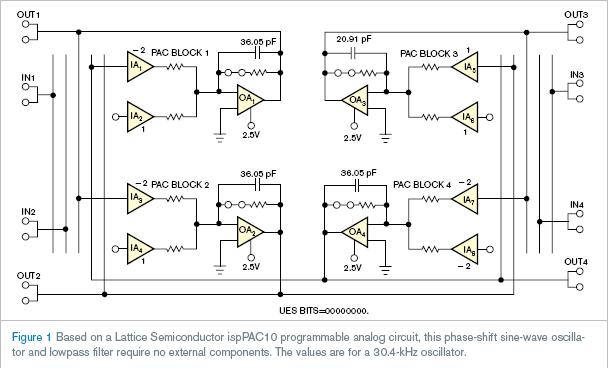
ispPAC10内部电阻固定在250 kΩ标称值上,所有电容由用户在1.07到61.59 pF之间选择。图1表示ispPAC10内部1、2和4模块被连接成级联的三个一阶低通滤波器,形成经典相位偏移RC振荡器。改变电容值产生超过18到130kHz范围的振荡频率。每个PAC模块增益被设置成2,从而获得-8的回路增益,这是振荡器的Barkhausen条件需要的(参考文献2)。配置模块3,一阶低通滤波器减少了振荡器输出的THD(总谐波失真)。模块3的电容值使滤波性能达到最优化,由此造成相位偏移不同。

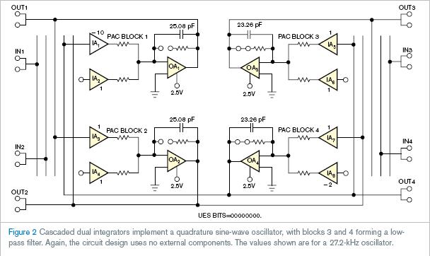
图2中电路描述了双积分器回路形成经典的求积RC振荡器。电路振荡器频率跨越从12到126 kHz,依靠模块1、2形成积分器的时间常数。理论上,每个积分器增益本该有个统一的绝对值,但实际上,ispPAC给出详细说明除了反向积分器,模块1中产生稳定的正弦信号所需要的至少-4增益。电路使用-10的增益。ispPAC10设备的两个附加模块形成能够降低输出THD的二阶低通滤波器。在两个振荡器电路中,改变低通滤波器增益,以便在所有频率的电路输出都可以传递特殊的电压,例如1V峰峰值。

表1和表2分别包含相位偏移、求积振荡器器件和输出特性的概要。电容值CN以频率f0在振荡器n次PAC模块中使用。设计使用Tektronix TDS1002数字振荡器的FFT功能,测量THD和中心频率f0,即-20 dB水平下每个输出频率的频谱线宽度。


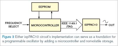
图3说明了基于ispPAC振荡器的微处理器对不同频率的动态重置的应用。非易失性存储器存储每个ispPAC10电路模块特殊频率的电容和增益值。数据传输通过ispPAC10的串行测试存取口接口,使用IEEE 1149.1 JTAG标准协议进行传输。

英文原文:
Programmable analog circuits yield single-chip sinusoidal oscillators
Internally programmed low-pass filters yield classic RC oscillator.
Stefano Salvatori and Paolo Lorenzi, University of Rome, Rome, Italy; Edited by Brad Thompson and Fran Granville -- EDN, 1/19/2006
Programmable-logic devices provide a popular method of implementing complex functions in digital designs.
Although manufacturers don't yet offer analog circuits whose complexity compares to VLSI digital circuits, field-programmable analog circuits are enjoying extensive use in signal-conditioning and filtering applications. Based on CMOS-operational-transconductance and switched-capacitor amplifiers, these devices offer a convenient approach to relatively complex design problems. Lattice Semiconductor's (www.latticesemi.com) ispPAC10 in-system-programmable analog circuit and its accompanying PAC Designer software offer a convenient method of circuit design and verification (Reference 1). This Design Idea presents two simple sinusoidal oscillators based on the ispPAC10.
Resistors within the ispPAC10 are fixed at a nominal 250 kΩ, and all capacitors are user-selectable from 1.07 to 61.59 pF. Figure 1 shows an ispPAC10 with its internal blocks 1, 2, and 4 connected as a cascade of three first-order lowpass filters to form a classic phase-shift RC oscillator. Altering the capacitors' values produces oscillation frequencies over a range of 1
8 to 130 kHz. Each PAC block's gain is fixed at a factor of two to obtain a loop gain of –8, which Barkhausen's condition for oscillation requires (Reference 2). Configured from Block 3, a first-order lowpass filter reduces the THD (total harmonic distortion) on the oscillator's output. The values of capacitors in Block 3 are optimized for filtering performance and thus differ from those of the phase-shift stages.
The circuit in Figure 2 describes a two-integrator loop that forms a classic quadrature-RC oscillator. The circuit's oscillation frequency spans 12 to 126 kHz and depends on the time constants of the integrators that blocks 1 and 2 form. In theory, each integrator's gain should have an absolute value of unity, but, in practice, ispPAC allows specification only of inverting integrators, and producing a stable sinusoidal signal requires a gain of at least –4 in Block 1. The circuit uses a gain of –10. Two additional blocks of the ispPAC10 device form a second-order lowpass filter that decreases the output's THD. In both oscillator circuits, you can alter the lowpass filters' gain so that the circuit's outputs deliver specific voltages, such as 1V p-p, at all frequencies.
Table 1 and Table 2, respectively, contain summaries of the phase-shift and quadrature oscillators' components and output characteristics. CN refers to the value of the capacitor used in the nth PAC block for oscillation at frequency f0. The design uses a Tektronix TDS1002 digital oscilloscope's FFT function to measure THD and the spectral line width of each output frequency at a level of –20 dB with respect to the central frequency, f0.
Figure 3 illustrates the application of a microcontroller to dynamically reconfigure an ispPAC-based oscillator for specific frequencies. The nonvolatile memory stores frequency-specific capacitance and gain values for each of the ispPAC10's circuit blocks. Data transfers occur using the IEEE 1149.1 JTAG-standard protocol through the ispPAC10's serial test-access-port interface.
References
PAC Designer software, www.latticesemi.com.
http://jlnlabs.imars.com/spgen/barkhausen.htm.

